![]()
by Andrew S. Huang, 9/14/96
Introduction
FPM DRAM, EDO DRAM, CDRAM, EDRAM, RDRAM, SDRAM, SGRAM, VRAM, WRAM, SRAM, SSRAM, SIMM, DIMM, DIP...
Do you know what all of these acronyms mean? Better yet, do you know the features of all these architectures? Well, before writing this FAQ, I was not familiar with most of these acronyms. In today's fast-paced industry with marketeers trying to gain product distinction and price premiums, the proliferation of acronyms is sometimes intimidating. I hope you find this FAQ as edifying and fun as I found it to write.
As a note from someone watching on the sidelines, the recent crash in DRAM prices indicates just how much DRAM manufacturers were inflating their prices. Even though DRAM prices dropped from upwards of $30 a Meg to around $5 a Meg, DRAM manufacturers are still making a small profit! A number of market factors were driving toward this crash; some of it is because the introduction of EDO and SDRAM forced FPM prices down to remain competitive, and some if it is because of the burgeoning demand for DRAM as new OSes and applications become less efficient and start chomping up more memory. Some of it is because of better process technology developed because DRAMs are getting denser. The DRAM market tends to be very elastic and prices volatile. Although EDO is the hottest stuff out right now, keep an eye on SDRAM. Make sure your motherboards support it as an upgrade, because it will probably be the Next Big Thing.
Acknowledgements, up front: most of the information presented in this
FAQ is lifted directly from databooks and magazine articles. I will cite
sources as I use them. Most pictures are scans from magazines, or lifted
from on-line databooks (thank you Micron!)--no, I didn't draw 'em myself.
If anyone finds material in this FAQ objectionable because of copyright,
send bunnie@mit.edu email, and
I'll find a suitable replacement.
![]()
DRAM
Overview
So, just what is DRAM? DRAM stands for:
The breakdown of this acronym hints at the workings underneath--some form of decaying storage, some form of addressable array. The fundamental element of a DRAM is a single capacitor-transistor element which stores 1 bit of information:
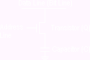
C is on the order of 1 fF (10e-15 F); at 1.6e19 electrons / coulomb, that is only about 40,000 electrons! Thus, even though the transistor has a fairly high off resistance of a few teraohms (10e12 ohms), the time constant for this circuit is on the order of milliseconds (typically tens to hundreds of milliseconds for modern designs). Also, when dealing with such tiny numbers, correctly sensing the presence or absence of charge is quite a challenge. DRAM arrays use special amplifiers, called sense amps, to detect the state of the capacitor. Once a bit has been read, it must be refreshed since reading pulls a lot of charge out of the capacitor. DRAM cells are so sensitive that stray alpha particles can induce errors (called soft errors by DRAM mfgs). I once heard that some nuclear scientists were using a massive array of DRAM chips as particle detectors! When designing with DRAM, keep in mind that it is primarily an analog part, and is quite sensitive to noise and power supply fluctuations.
Well, with a few million of these sensitive devices on a single die, one can imagine that support circuitry is required. Here is a block diagram of a typical, bare-bones DRAM array (1Megx4 FPM):
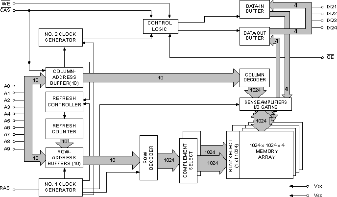
Picture from Micron on-line datasheet
The important features to glean from this diagram are:
Now that the basic DRAM structure has been introduced, I will discuss what makes the different flavors of DRAM significant. I will approach this from two directions: that of architecture, and that of timing.
Fast Page Mode DRAM is the vanilla DRAM as of June 1996, and is rapidly being replaced by other faster technologies. By the time you read this, FPM DRAM will probably be obsolete. Still, it enjoyed a huge popularity for a few years, so it is the standard against which all other DRAM architectures are compared.
Each normal DRAM access requires two address cycles, one for row address, and one for column address. A fast page mode DRAM access consists of a sequence of accesses where only the first access specifies both row and column addresses; the remainder specifies just a column address (the row address is implicity the same). This asymptotically reduces access time by 50%. If one thinks of each row of a DRAM as a page of data, one can see the etymology of the fast page nomenclature.
FPM works in a real system because there is some spatial locality of data access patterns--in general, if you grabbed data from one area, you are likely to grab more data from that area. If data access patterns were completely random, FPM would only perform marginally better than normal DRAM. This situation is analogous to someone looking for words in a dictionary; looking for words that happen to be on the same page is faster than looking for words on different pages.
Of course, in order to take advantage of FPM, the system must be designed to utilized FPM...replacing normal DRAM with FPM DRAM offers no speed improvement without system reconfiguration.
The following timing diagram illustrates a typical non-FPM DRAM read access:
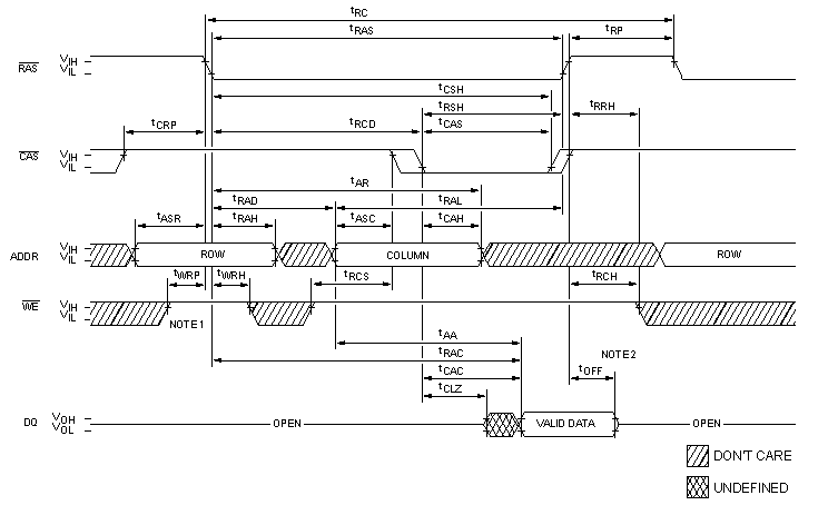
Picture from Micron on-line datasheet
Notice that in order to get a single piece of data, both a row and a column address must be provided.
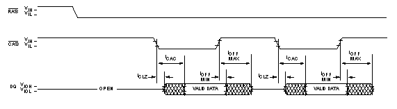
Picture from Micron on-line datasheet
The above picture is my lame attempt to find an image which illustrates an FPM access. Sorry, I don't have the time just now to draw one up with all the signals illustrated, but this might give you the idea--notice how the CAS (column address strobe) happens twice while the RAS (row address strobe) is held low the entire time. If the addresses were drawn in, you would see that the row address is supplied only once at the beginning of the cycle, while two column addresses are supplied.
Around 1994, a new family of DRAM entered the market--EDO. EDO is architecturally identical to FPM DRAM; in fact, it is so similar that often times one manufacturer's chips labelled as EDO have the same silicon die as their chips labelled as FPM. The dies are differentiated at the last stage (packaging) with a fuse or die bond option. Thus, manufacturers can manufacture a single lot of dies and meet the changing demand for EDO and FPM as market conditions change, and reap extra profits when demand for EDO is high.
EDO stands for Extended Data Out. The reason for this name becomes apparent if one compares the timing characteristics of EDO vs. FPM DRAM.
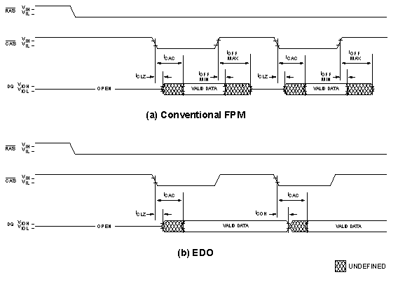
Picture from Micron on-line datasheet
As one can see, in EDO, the time period for which data is valid is longer than the time period for FPM, hence extended data out. The technical difference is that the data buffers aren't turned off with CAS; instead, data remains valid until the next piece of data is available. Thus, this clever hack only requires modifications to the data buffer circuitry and a few other control functions.
EDO wins because the amount of time required for data to be valid at the system level is constant. If a system using FPM requires data to be valid for 10ns but the time between accesses is 40ns, then a single access takes 50 ns. With EDO, there is less overhead, so the time between accesses is cut down. Thus, the time between accesses may be reduced to 20ns for a total access time of 30ns. Note that these numbers are only illustrative; in fact, they're pretty far off from what's really out there.
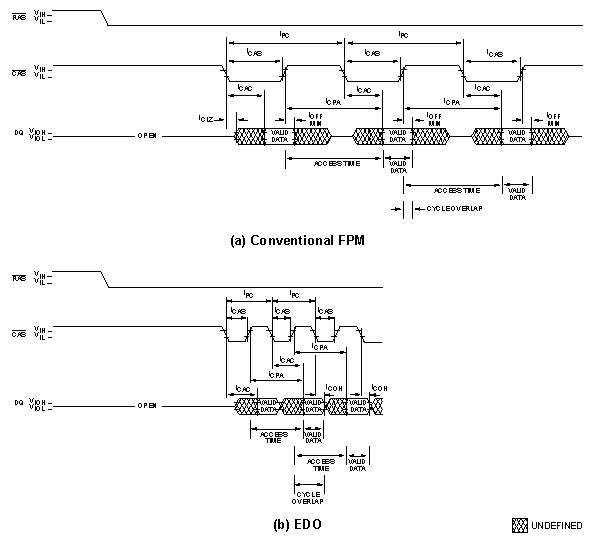
To really get a feel for what EDO buys at the system level, the following diagram compares the timing of a system designed to take full advantage of EDO and a system designed for FPM only:
Picture from Micron on-line datasheet
Notice how the period of valid data remains the same between the systems. Hence, all the extra time for which data is valid in an EDO access can be lopped off and the overall access time shortened.
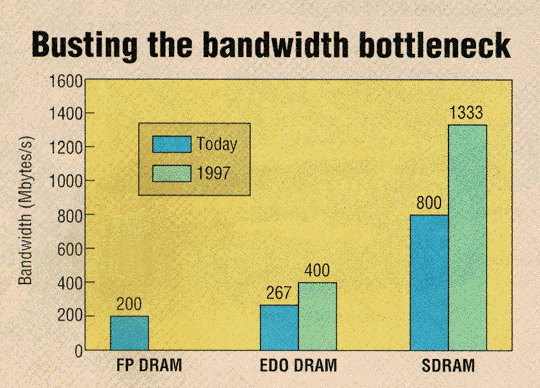
Picture from Computer Design web page.
Ooops...ran out of time. I'll write more later. If you wanna know more about other DRAM formats, bother me (bunnie@mit.edu) and I'll write some more!
Actually, since this page is getting quite old and I've had way too much to do, check out Tom's Hardware Page if you want to find out more about the current state of the art in commodity DRAM technology. When I get to the chapter in my thesis about DRAM technology, I'll be sure to mirror more of that information to this page. =)
If you have comments, corrections, or suggestions, email me at bunnie@mit.edu
![]()
This page created with Netscape Navigator Gold (thanks, Netscape!)